Comparison of the processors of the Intel 6th generation. Intel processors generations: description and characteristics of models. ▍Multimedia and graphics
Moscow, November 19, 2015 - Intel submitted 6 generation intel processors® Core ™ in Russia and other CIS countries. As a new generation of processors will change the user experience, Intel experts and corporation partners told. The highest speed, new integrated 3D graphics, fast and efficient video processing - only a brief list of advantages of new processors, the details of which were presented by engineers, architecture specialists and partners.
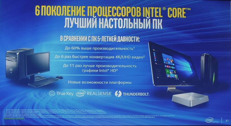
Intel® Core ™ 6-Generation Processors - the best for the whole history Intel - at high performance orbit and energy efficiency
For one day, the Moscow club Art Hall turned into a flying center. Engineers, architecture specialists and partners, which reported on readiness for the launch of devices that take the user to a new performance orbit of productivity are participants in the bright show. A presentation was opened by the solemn launch of a new generation of processors decorated for the start of the spacecraft.
Bernadett Andrietti, Vice-President of Intel Corporation and Intel Marketing Director in Europe, in the Middle East and Africa, announced the start of the PC Refresh campaign - the Intel, Microsoft joint action and leading PC manufacturers dedicated to the contemporary computer features. Acquired 4-5 years ago, computers are slowly turned on, do not support all functionalityAvailable to users today, their batteries lack for a long time. That is why Intel Corporate PC Refresh, the basic idea of \u200b\u200bwhich is to tell users about new opportunities. modern gadgetswhich are not capable of old devices.

The 6th generation processors presented Dmitry Konash, the Intel Regional Director in Russia and other CIS countries. "Today, users expect from their devices of the highest performance and lower power consumption," said Dmitry Konash. - Both of these tasks decide new processors, the best in the history of Intel, withdrawing computers to a new level of productivity, energy efficiency and new opportunities to implement the creative potential of users. "
Mikhail Flowers, an Intel architecture specialist in Russia and other CIS countries, noted a number key features The Intel® Core ™ processor of the 6th generation, thanks to which the Corporation has made another big jump in energy efficiency. The performance of the performance of the processor cores while reducing power consumption is carried out using the Intel® Speed \u200b\u200bShift technology and the integration of new hardware functions on a processor crystal, such as Image Signal Processor (ISP). With Intel® Speed \u200b\u200bShift Technology, the processor is able to independently manage the modes of its work. This reduces the reaction time to load change up to 30 times and increase overall productivity Systems by 20-45%.
The 6th generation Intel® Core ™ processors are based on the industry-leading 14-nanometer manufacturing process and provide up to 2.5 times higher performance, 3 times a longer battery life and 30 times higher quality graphics for smooth Works of games and video playback compared to computers purchased 5 years ago. In addition, they can have 2 times lower thickness and 2 times less weight, can faster switching to the operating mode and work without recharging for a whole day.
For users, this means improved visual characteristics for games, photos and videos. The new technology Intel Speed \u200b\u200bShift increases the dynamism of work mobile systems In order for users, for example, can apply filters for editing photos up to 45% faster. The ability to manage RealSense cameras will make realistic 3D-selfie, scan items and print them using 3D printers, as well as easy to replace the background during communication in video chats. The new platform also supports technology. Intel Widi. and Pro Widi, allowing users to transfer an image from computers to televisions, monitors or projectors without using wired connections.
Dmitry Khalin, director of the Microsoft Technological Policy Department in Russia, spoke about strategic cooperation of companies, noting that new Intel® Core ™ processors are optimized for working with Windows * 10, which provides them with new functionality and reliable protection. For example, devices with Intel RealSense camera and windows support Hello allows users in a secure mode to enter the system using the feature feature feature.
"Microsoft fruitfully cooperates with Intel is not one decades. Together we do our best to provide users wide selection Extremely powerful, fast and convenient devices. We recently released our most modern operating system Windows 10. We are confident that in combination with the newest processors Intel It will allow customers around the world to more effectively fulfill any personal and working tasks, "says Dmitry Khalin.
Vlad Zakharov, Marketing Manager Asus Russia, introduced the 8th generation Intel® Core ™ Records. New processors demonstrate a number of significant improvements in the field of computational technologies. Thanks to them, a record result was installed in Super PI 32M team members Team Russia as part of the event in Moscow ASUS OC Summit 2015. The Intel® Core ™ i7-6700K processor managed to dispersed to the frequency of 6593 MHz on the ASUS motherboard Rog Maximus. VIII EXTREME, and the RAM at the same time worked at a frequency of 3733 MHz with Townings CL15 18-18-28 1T. The resulting result of 4 minutes 42.141 seconds was the first among the results on the Core i7-6700K in the world, ahead of the previous leader for more than 6 seconds.
Throughout the event, an affiliate exhibition worked, where devices were presented on the Intel® Core ™ Core ™ processors. ASUS, DELL, LENOVO, MSI and other vendors have demonstrated all varieties of form factors: laptops, incl. Gamers, desktops, monoblocks, mini-pc.
Guests of the presentation could also get acquainted with other solutions of Intel: Cappasity Easy 3D Scan and Aldebaran Nao. CapPasity Easy 3D Scan is a software product for ultrabooks with an Intel RealSense 3D camera, with which you can create high-quality 3D models. The Aldebaran Nao robot is a companion robot, equipped with Intel® Atom ™. He independently focuses in space, has 25 degrees of freedom of movement, the ability to take small objects, shoot video, take photos and send them to the network.
In August 2015, the 6th generation of computing chips from Intel was presented - Skylake. The processor relating to this generation received a substantially recycled architecture, which allowed to increase the speed by 10-15% compared to the CPU of the previous generation under the code name Haswell. It is about them technical parameters, opportunities and species will go further.
Background appearance
Currently, every 2 years, Intel updates processor connectors. So, in 2013, the LGA1150 was released along with the Haswell Light CPU. This is the 4th generation of CPU based on the Core architecture. Then, a year later, Broadwell came to the Haswell chipam. This is the 5th generation of Core architecture CPU. Their difference is the renewed technological process that makes up 14 nm. But the processor part has not changed. Then to change 4-y and 5th family of chips based on the Core architecture from Intel in 2015, the 6th came already, which received the code name Skylake. The processor of any model of this generation is made according to a similar technological process - 14 nm (as well as Broadwell or 5th generation of the Core architecture). But at the same time, the architecture of the computational part was recycled, and this made it possible to obtain a certain increase in performance in 10-15%. Also, the semiconductor crystal nutrition subsystem was recycled. Now the CPU voltage regulators are made on the motherboard. Such an engineering approach made it possible to maintain practically no changes to the subsystem of nutrition, but at the same time improved the accelerated potential of the central processor.
Socket and System Logic Sets
It is the LGA1151 socket that is intended for the installation of any Skylake's desktop chip. The new generation processor in this case is designed to install in a new connector and incompatible with the CPU of the previous generation. Also to support the new generation of central processors, a new generation of sets was issued system logic. The most modest among them from the position of the functional set is H110, users say. But at the same time, the cost of him is appropriate. It is perfect for the system of budget, elementary level. The most functional and most expensive in this case, the set of logic is z170. The key difference from all other chipsets is the possibility of overclocking the CPU with a unlocked multiplier (it is precisely on the installation of such CPUs, it is oriented), a built-in graphics accelerator and even RAM. This is an excellent solution for creating the most productive PC. The remaining variants of H170, B170, Q150 and Q170 are intermediate between the two previously reduced system logic sets, and their main purpose is the assembly of an average price level PC and exactly the same speed.

Technical features
As noted earlier, the kernel processor Skylake. It was significantly recycled, and due to this, an additional increase in speed was obtained. But most of his part did not undergo significant changes. This is the first level of the cache. Its total volume for one block is 64kb, which are divided into 2 parts of 32 kb for data and instructions. The second level no longer has such a separation, and its volume is 256 Kb. The third level of the cache is common to all CPU computing resources, and its volume depends on the specific model: from 2 MB for Celeron processors and up to 8 MB for i7. The technical process, as noted earlier, did not change in comparison with the predecessors - 14 nm. The chipset, as in the previous generations of processors, is part of its semiconductor crystal. That is, the composition of the CPU, in addition to the computing part and the graphics accelerator, also includes a PCI-Express controller and a two-channel RAM controller. The latter can work with DDR4.
Entry Solutions
Skylake entry levels are chips of model series Celeron and Pentium. Physically and programmatically on these semiconductor crystals are only 2 computing modules and the same amount of data processing streams. The most accessible cost is the first of them, but at the same time, they are significantly lower. More high level The performance of the Pentium line chips is provided by increased and enlarged 3 level cache. Also, in the latter case, a more productive graphic subsystem HD Graphics with an index 530 is used, while Celeron is equipped only with a decide with the designation 510. Exception in this regard is the Pentium G4400 with a shortened version of the built-in video card 510. A Celeron G3900T model is held separately in this family with The thermal package is only 35W and a reduced clock frequency of 2.6 GHz. Otherwise, more detailed specifications of Celeron and Pentium processors of the 6th generation are shown in the table.
Model and processor index | Cash 3 level, MB | Fixed chip frequency, GHz | Number of chip / stream nuclei | Thermal package, w | HD Graphics Video Card Model |
||
Medium segment
In the middle segment, this generation of CPU is represented by the Core i3 lineup processors. Total to this niche currently applies 6 chips. All of them include 2 physical computing blocks and 4 software streams. That is, in these processors there is support for branded technology from Intel, which calls Hypertrading.

It is this feature that allows you to increase the number of information processing streams by 2 times programmatic level. But the support of TurboBoST technology speech in this case does not go, and the frequency of the processor is fixed. Two representatives of this family with 6100T and 6300T indices have reduced clock frequencies and a reduced thermal package of 35 watts. These are energy-efficient solutions aimed at creating compact computer Systems. One chip with marking 6098R is equipped with less productive graphic system HD Graphics with index 510. All processors of the 60xx and 61xx series have 3 MB of 3-level cache, and the series 63xx - 4 MB. Integrated video scorer in all other cases has an index 530. More detailed features All six-generation I3 processors are listed in the table below text.
Processor name | Third-level cache, mb | Processor clock frequency, GHz | The number of real nuclei / software streams | The values \u200b\u200bof the thermal package, W | Cost, USD. | HD Graphics Accelerator Model |
|
Most productive quad-core solutions
The most massive semiconductor solution in this case is the processor Intel Core I5. Skylake-architecture In this case, 9 models of chips are represented at once. All of them have 4 computing kernels. Two models with 6685R and 6585R indexes have an improved graphic subsystem of HD Graphics model 580, one, 6402p, less productive - 510. Three chips 6400T, 6500T and 6600T are energy-efficient solutions with reduced frequencies and a reduced heat package. The remaining 6400, 6500 and 6600 processors are standard representatives of this line of devices. More detailed technical specifications of the CPU i5 of this generation are shown in the table.
Marking | Cash 3 level, MB | MIN / MAX frequency range, GHz | Number of physical nuclei / information processing streams | The meaning of the thermal package, W | Price current, USD | Video Aaclator HD Graphics. |
|
Eight-step chips with maximum speed
Any Core Skylake related to the I7 line has full set All sorts of technologies (Hypertrading and TurboBoost). It can handle data in 8 threads and dynamically change its frequency.

In terms of performance, these processes lose only the most expensive solutions for computer enthusiasts, which are unlocked by the frequency multiplier, and due to this, a significant increase in speed can be obtained. At the moment, the composition of this line includes only 3 chips, and their specifications are shown in the table below. One of the models has a 6700T index, and this is an energy efficient CPU for assembling high-performance compact systems. The second is 6785r. It is equipped with an improved graphic accelerator model with an index 580. And the last, 6700 is a typical flagship with a blocked multiplier and maximum speed (except for chips for enthusiasts).
CPU designation | Kesh 3 level, MB | Frequency MIN / MAX Formula, GHz | Number of nuclei / information processing streams | Declared thermal package, w | The stated value, USD | Video adapter HD Graphics. |
|
Products for computer enthusiasts
As in the previous generations of Core processors, only 2 models of chips have a unlocked multiplier. The first one is 6600K. This is a typical quad-core I5 \u200b\u200bprocessor. Skylake-architecture has a shared overclocking potential. In the presence of a high-quality cooling system, its frequency can be increased without any problems with 3.9 GHz to 4.6-4.7 GHz with a simple raising of the multiplier. If you also change the voltage on the semiconductor crystal of the processor, then it is possible to obtain even 5.0 - 5.1 GHz.

The second representative of this family is 6700K, which is already refer to the I7 line. He has parameters identical to all other chips of this model range. The key difference that specialists noted is a unlocked multiplier. Well, the frequencies that can be obtained during acceleration are similar to 6600K. Their technical specifications are shown in Table 5.
Reviews. RESULTS
Users claim that a decent continuation of the preceding generations of chips of the Skylake CPU. The processor of this family, in their opinion, has improved both from the position of speed and from the energy efficiency position.

The life cycle of this platform only begins, and according to Intel, it will be even relevant to the next 3 years. So it's time to buy a new high-performance and energy efficient personal computer.
One day one great sage in the captain's chains said that a computer could not work without a processor. Since then, everyone considers his duty to find the same processor, thanks to which his system will fly as a fighter.
From this article you will learn:
Since we simply cannot cover all the well-known sciences of chips, we want to focus on one interesting family of the genus Intelovichi - Core I5. Very characteristics of interesting and productivity are good.
Why is this series, not i3 or i7? Everything is simple: excellent potential without overpayment for unnecessary instructions, which sinters the seventh ruler. Yes, and cores more than in Core i3. You will quite naturally begin to argue about support and find yourself partially right, but 4 physical cores are able much more than 2 + 2 virtual.
History series
 Today on the agenda we have a comparison of Intel Core i5 processors different generations. Here I would like to touch on such pressing themes like a heat pump and the presence of solder under the lid. And if there is a mood, then also foreheads with each other, especially interesting stones. So, let's go.
I want to start with the fact that the desktop processors will be considered exclusively, and not options for the laptop. Comparison of mobile chips will be, but another time.
The output frequency table is as follows:
| Generation | Year of issue | Architecture | Series | Socket | Number of nuclei / streams | 3 level cache |
| 1 | 2009 (2010) | Hehalem (Westmere) | i5-7xx (i5-6xx) | LGA 1156. | 4/4 (2/4) | 8 MB (4 MB) |
| 2 | 2011 | Sandy Bridge. | i5-2xxx | LGA 1155. | 4/4 | 6 MB |
| 3 | 2012 | Ivy Bridge. | i5-3xxx | LGA 1155. | 4/4 | 6 MB |
| 4 | 2013 | Haswell. | i5-4xxx | LGA 1150. | 4/4 | 6 MB |
| 5 | 2015 | Broadwell. | i5-5xxx | LGA 1150. | 4/4 | 4 MB |
| 6 | 2015 | Skylake. | i5-6xxx | LGA 1151. | 4/4 | 6 MB |
| 7 | 2017 | Kaby Lake | i5-7xxx | LGA 1151. | 4/4 | 6 MB |
| 8 | 2018 | Coffee Lake | i5-8xxx | LGA 1151 V2. | 6/6 | 9 MB |
2009
 The first representatives of the series saw the light in the distance in 2009. They were created on 2 different architectures: Nehalem (45 Nm) and Westmere (32 Nm). The most vivid representatives of the line should be called i5-750 (4x2.8 GHz) and I5-655K (3.2 GHz). The latter additionally had a unlocked multiplier and the possibility of overclocking, which spoke about its high performance in games and not only.
The differences between architectures lies in the fact that Westmare is built on the norms of the technical process of 32 nm and have 2 generation shutters. And they have less power consumption.
2011
This year, the second generation of processors saw the light - Sandy Bridge. Them distinctive feature It was the presence of the built-in video card in Intel HD 2000.
Among the abundance of models I5-2XXX, I would especially want to highlight the CPU with an index 2500K. At one time, it produced a real extension among gamers and enthusiasts, combining the high frequency of 3.2 GHz with support for Turbo Boost and low cost. And yes, under the lid there was a solder, not a thermalcaste, which further contributed to the qualitative acceleration of the stone without consequences.
2012
 The ivy bridge debut brought the 22-nanometer technical process, higher frequencies, new DDR3, DDR3L controllers and PCI-E 3.0, as well as USB 3.0 support (but only for i7).
Built-in graphics evolved to Intel HD 4000.
Most interesting decision This platform has become a Core i5-3570K with an unlocked multiplier and a frequency of up to 3.8 GHz in the boosa.
2013
The Haswell generation did not bring anything supernatural except the new LGA 1150 socket, the AVX 2.0 instruction set and the new HD 4600 graphics. In fact, the whole focus was made on energy saving, which companies managed to achieve.
But as a spoon of the fly, the replacement of the solder on the thermal interface is, which greatly reduced the acceleration potential of the top i5-4670k (and its updated version of 4690K from the Haswell Refresh line).
2015
In essence, it is the same Haswell transferred to the architecture of 14 nm.
2016
 The sixth iteration under the name Skylake brought the updated LGA 1151 socket, support for RAM type DDR4, IGP 9th generation, instructions AVX 3.2 and SATA Express.
Among the processors it is worth highlighting I5-6600K and 6400T. The first was loved for high frequencies and unlocked multiplier, and the second for low cost and extremely low heat dissipation of 35 W despite supporting Turbo Boost.
2017
Era Kaby Lake is the most controversial, because there was absolutely nothing new to the segment of desktop processors other than native USB support 3.1. Also these stones are completely refused to run on Windows 7, 8 and 8.1, not to mention older versions.
The socket remained the same - LGA 1151. Yes, and the set of interesting processors has not changed - 7600K and 7400T. The reasons for people's love are the same as Skylake.
2018
 GOFFEE LAKE processors are radically different from their predecessors. To change the four cores, it came 6 that only the top versions of the i7 series X could be allowed to be allowed. The size of the L3 cache increased to 9 MB, and the heat pump in most cases does not exceed 65 watts.
From the whole collection, the model I5-8600K is considered the most interesting for the possibility of overclocking up to 4.3 GHz (though only 1 nucleus). However, the audience prefers I5-8400 as the most inexpensive "entrance" ticket.
Instead of results
If we were asked what we would suggest the lion's share of gamers, we would say without knocking that I5-8400. The benefits are obvious:
- the cost is below $ 190
- 6 full-fledged physical cores;
- frequency up to 4 GHz in TURBO BOOST
- heat pipe 65 W.
- complete fan.
Additionally, you do not have to pick up "defined" rAMAs for Ryzen 1600 (the main competitor to the word), and the core themselves in Intel. You are denying additional virtual flows, however, practice shows that in games they only reduce the FPS, not bringing certain adjustments to the gameplay.
By the way, if you do not know where to buy, I recommend paying attention to one very popular and serious (believe me, he is known to someone and familiar) - at the same time you can navigate at the prices of i5 8400, periodically, and more precisely, very often I use this resource yourself, I use this resource To decide on whom it is more profitable to apart.
In any case, to solve you. Before new meetings, do not forget to subscribe to the blog.
And also news for those who follow (solid-state discs) - it rarely happens.
On August 5, Intel announced two new Intel Core 6th Generation Processors (Skylake code name): Core i7-6700k and Core i5-6600K. In addition, the new Intel Z170 chipset was announced, and leading maternal manufacturers simultaneously announced their solutions based on the Intel Z170 chipset.
We have the opportunity to test Intel Core i7-6700K and Core i5-6600K processors and compare them with the processors of the previous generation.
SkyLake processors
This article is preparing what is called, in the avral mode, before the announcement new platformWhen official information relative to new processors was a bit. Therefore, some questions regarding new processors we will leave out of consideration. In particular, we will not consider the microarchitecture of new processors and the peculiarities of the new Intel graphics core. Intel is going to inform the details of the new microarchitecture within the framework of the IDF 2015 exhibition, which will be held at the end of August.
So, let's start with the fact that the new family of the 8th generation Intel Core processors is known under the code name Skylake. These are processors performed on a 14-nanometer process. Recall that Intel provides its processors in accordance with the Tick-Tock Rule (TIK-like), which was invented in Intel itself. The meaning of the rule is that once every two years the processor microarchitecture is changing, and the process of production changes every two years. But the change of microarchitecture and the technical process shifted relative to each other for a year. That is, once a year, the technical process changes, then, after a year, the microarchitecture changes, then again in a year, the technical process changes, etc., someone has occurred to associate such periodic shifts of microarchitecture and the process with the movement of the pendulum in the clock and There was a "Tick-Tock" rule. Moreover, the change in the process is the "Tick" cycle, and the microarchitecture change is the Tock cycle. It is impossible to say that Intel has strictly withstands the time frame of this rule, but, in any case, trying to adhere to this rule.
So, the processors of the previous generation, known for the code name Broadwell, marked the transition to the 14-nanometer technical process ("Tick"). These were processors with Haswell microarchitecture (with minor improvements), but manufactured according to a new 14-nanometer technical process.
Accordingly, the SKYLAKE processor family is the "Tock" cycle processors, that is, they are produced by the same 14-nanometer technological process that Broadwell processors, but they have a new microarchitecture.
As already noted, on August 5, Intel announced only two models of the Skylake family processors for desktop PCs. But this, of course, does not mean that the Skylake family will consist of only two models. According to unofficial information, at the end of August - early September, 8 more models of Skylake processors for desktop PC will be announced. Yet we are talking Only two models that have a unlocked multiplication factor (K-series).
In general, the Skylake processor family will include four separate series: Skylake-S, Skylake-H, Skylake-U and Skylake-Y. Skylake-H, Skylake-U and Skylake-y series processors will have BGA-execution and are focused on laptops, tablets and monoblocks. Moreover, the processors of these series are SOC (SYSTEM-ON-CHIP), that is, they do not require a separate chipset (Platform Controller Hub, PCH).
Skylake-S series processors are focused on desktop systems, which have LGA-execution and work only in conjunction with a single-chip chipset (PCH). It is about these processors that we will continue to talk.
The Skylake-S series processors have a LGA1151 connector and, of course, are compatible only with motherboards based on new Intel chipsets 100th series.
One of the innovations in the SkyLake-S processors is that the processor voltage regulator (Fully Integrated Voltage Regulator, FIVR), which in the Haswell processors was located inside the processor itself (and the fact that the company Intel was very proud of), was now issued for The limits of the processor and is located on the motherboard.
Another innovation is that the SkyLake-S processors will support the DDR3L memory (with reduced supply voltage), and the DDR4 memory. Moreover, memory controllers are two-channel and support up to two memory modules per channel.
In the same way as in the Haswell and Broadwell processors, in the Skylake processors there is a PCI Express 3.0 controller (PCIE 3.0) on 16 ports that can be used to organize slots for discrete video cards or extension boards.
New SKYLAKE-S processors have a new graphics core. In the processors for SKYLAKE-S desktop systems, only the SkyLake-GT2 graphics core will be used, and in the family of processors for laptops there will be models with graphic kernels Skylake-GT2, Skylake-GT3E and Skylake-GT4E.
Recall that in graphics nuclei, in the code designation of which the letter "E" (GT3E, GT4E) appears, an additional EDRAM memory is used (Embedded DRAM). Such a memory appeared in the top models of Haswell mobile processors, and there was no in the Haswell processors for desktop PCs. The EDRAM memory was a separate crystal, which was located on one substrate with a processor crystal. This crystal has also been known for crystalwell code.
IN mobile processors Haswell EDRAM memory had a size of 128 MB and was manufactured using a 22-nanometer process. But the most important thing is that this EDRAM memory has been used not only for the needs of GPU, but also for the computational cores of the processor itself. That is, in fact, Crystalwell was an L4 cache separated between GPU and processor computational cores.
In the Broadwell processor family for desktop PC, there is also a separate EDRAM memory crystal with a size of 128 MB, which acts as a L4 cache and can be used by the graphics core and processor computing cores. Moreover, the EDRAM memory in the 14-nanometer processors of Broadwell is exactly the same as in the top mobile processors of Haswell, that is, it is performed on a 22-nanometer process.
In the processors of the SKYLAKE-S family, the EDRAM memory will not be used.
In general, about the graphic kernel in the SkyLake-S processors, the data at the time of writing this article was practically absent. It is only known that in the Core i7-6700K and Core i5-6600K and Core i5-6600K models, the graphics of the Intel HD Graphics 530 (code name Skylake-GT2). As for the number of executive devices (EU), then there is no information about it. It is only known that in the top version of the new graphics core Intel (apparently, we are talking about the GT4 kernel) will be 72 EU.
Now we will list those characteristics of Intel Core i7-6700K and Core i5-6600K processors, which were known at the time of writing:
Both processors (Intel Core i7-6700k and Core i5-6600K) have a unlocked multiplication ratio, that is, they are focused on overclocking. The processor multiplication factor may vary in the range from 8 to 83.
We also note that the Intel Core i7-6700K processor is the top model in the SkyLake-S family.
Intel Chipsets 100th Series
Simultaneously with new 14-nanometer processors SkyLake-S Intel announced the new Intel chipset of the 100th series (SUNRISE POINT code name). On the 5th of August, only one chipset was presented: Intel Z170. Later, in early September, a few more models of the chipsets of the 100th series will be presented. In total, the Intel's 100th series chipset family will include six models: Z170, H170, H110, Q170, Q150 and B150.
Models Q170 and Q150 are focused on the corporate market and go to replace the chipsets Q87 and Q85, respectively.
Models Z170, H170, H110 are oriented to custom PC and replace the model Z97, H97 and H81, respectively. The B150 chipset is the replacement of the B85 chipset and is focused on the SMB sector of the market.
Note that if the Intel 9th \u200b\u200bseries chipsets practically did not differ from their predecessors, Intel's 8-series chipsets, then between the 100th series chipsets of the 100th series and the Intel's chipsets of the 9th series of differences are very significant.
Next, we consider the features of the Intel chipsets of the 100th series as a whole, without binding to a specific model, focusing on the top models of chipsets, in which everything is implemented at the maximum, and the features of each chipset are separately considering a little later.
To begin with, all Intel's 100-series chipsets now have a built-in PCI Express 3.0 controller (previously in the chipsets was the PCI Express 2.0 controller), and therefore you need to distinguish the PCIe 3.0 ports from the processor and from the chipset. As already noted, SKYLAKE processors have 16 PCIe 3.0 ports (PEG). The 100th series Intel chipsets allow combining these 16 PCIe 3.0 processor ports to implement various PCIE slot options. For example, Intel Z170 and Q170 chipsets (as well as their analogs of Intel Z97 and Q87) allow combining 16 PEG ports of PCIe 3.0 in the following combinations: x16, x8 / x8 or x8 / x4 / x4. Thus, on charges with Intel Z170 or Q170 chipset based on PCIe 3.0 processor ports, one slot PCIe 3.0 x16 can be implemented, two PCIe 3.0 x8 slots or one PCIe 3.0 x8 slot and two PCIe 3.0 x4 slots. Intel H170, B150 and Q150 chipsets admit only one possible combination of PEG ports: x16. That is, only one PCIe 3.0 X16 slot based on the PCIe 3.0 processor ports can be implemented on the boards with these chipsets.
Also, the Intel 100 series chipsets support two-channel DDR4 or DDR3L memory operation.
In addition, the Intel's 100th series chipsets support the possibility of simultaneously connecting up to three monitors to the processor graphic kernel (In the same way, as in the case of chipsets of the 9th series).
To communicate the Skylake processor, the Intel's chipset of the 100th series uses a new Tire DMI 3.0. Recall that in the Intel 9th \u200b\u200band 8th series chipsets, a DMI 2.0 bus with a 20 Gbit / s bandwidth in each direction (DMI 2.0 bus bandwidth corresponds to the PCI Express 2.0 x4 bus bandwidth). However, taking into account the fact that the PCIe 3.0 controller is now built in the 100th series chipsets, the use of DMI 2.0 bus to communicate the processor with the chipset would be illogical, since this tire could be a bottleneck. That is why in order to communicate the chipset with the processor, a more high-speed DMI 3.0 bus with twice by heavy throughput is used.
It is worth paying attention to the fact that in addition to the DMI 3.0 tire, no more connection between the processor and the chipset is provided. That is, there are no more FDI bus, which previously allowed to implement analog video output through the chipset. Thus, with the arrival of a new platform, the VGA connector goes into the past. If support for VGA and will be implemented on motherboards, then due to additional scheme Converting a digital video signal to analog. But it is unlikely, since it simply does not make sense.
As already noted, one of the main features of the new Intel's chipsets of the 100th series is that the PCI Express 3.0 controller is implemented. Moreover, in the top models of chipsets, up to 20 PCIe 3.0 ports (in Intel 9th \u200b\u200bseries chipsets, only up to 8 PCIE 2.0 ports were maintained).
In addition, as earlier, there is in new chipsets and an integrated SATA controller that provides up to six SATA 6 Gb / s ports.
Well, and, of course, the Intel RST (Rapid Storage Technology) technology is supported, which allows you to configure the SATA controller in the RAID controller mode (though not on all ports) with support for levels 0, 1, 5, and 10. The innovation is the fact Intel RST technology is now supported not only for SATA ports, but also for drives with PCIE interface (x4 / x2) (M.2 and SATA Express connectors). This option received the name Intel RST for PCIE Storage. Moreover, the Intel 100 series chipsets support Intel RST for PCIE Storage technology for three PCIe X4 / X2 interfaces that can be implemented as M.2 or SATA Express connectors. Also note that through the 100th series of the 100th series on the board can be implemented up to three SATA Express connectors.
The number of USB 3.0 ports in new chipsets has become greater. So, in the Intel 9 series chipsets (just as in the 8th series chipsets) there were only 14 USB ports, of which up to 6 ports could be USB 3.0, and the rest - USB 2.0. Intel's 100 series chipsets also have only 14 USB ports, but from them up to 10 ports can be USB 3.0, and the rest - USB 2.0. Note that one USB 3.0 port supports the OTG function (USB on-the-Go) (this has not previously previously). Theoretically, it allows you to directly link with each other two USB-HOST devices without the use of a special cable. However, it is not a fact that this feature uSB ports It will be possible to use in practice. It all depends on the manufacturer of the motherboard and the availability of the appropriate driver. For example, on the Asus Z170-Deluxe board, which we managed to test, the OTG function was not supported.
In the same way as in the Intel 9th \u200b\u200bchipsets and the 8th series, the 100th Series Intel chipsets implemented Flexible I / O technology, which allows you to configure high-speed I / O ports (PCIE, SATA, USB 3.0), Removing some ports and adding others. However, there is a significant difference between Flexible I / O technology in the Intel 9 / 8th series chipsets and this technology in the 100th series chipsets.
Recall that in the Intel 9 / 8th series chipsets, only 18 high-speed I / O ports could have. All high-speed chipset ports are numbered. Moreover, 14 ports were strictly fixed: these are four USB 3.0 ports, six PCIE 2.0 ports and four SATA ports 6 Gb / s. But four more ports can be reconfigured: two of them can be either ports of USB 3.0, or PCIE, and two more others - either PCIE, or SATA 6 Gb / s. In this case, the total number of PCI ports cannot be more eight.
The distribution diagram of high-speed I / O ports for Intel 9/8 series chipsets is shown in the figure.

In the Intel's 100th series chipsets, 26 high-speed I / O ports can be implemented (Intel's technical documentation, these ports are called High Speed \u200b\u200bI / O Lanes (HSIO)).
Six first high-speed ports (PORT # 1 - Port # 6) are strictly fixed. These are USB 3.0 ports. The following four high-speed chipset ports (PORT # 7 - Port # 10) can be configured either as USB 3.0 ports or as PCIE ports. And port port # 10 can be used and as network port GBE. That is, it is that the MAC controller of the network gigabit interface is embedded in the chipset itself, but here is the PHY controller (MAC controller in bond with a phy controller form a full-fledged network controller) can only be connected to a specific high-speed chipset ports. In particular, it can be ports Port # 10, Port # 11, Port # 15, Port # 18 and Port # 19.
Even eight high-speed chipset ports (PORT # 11 - Port # 14, Port # 17, Port # 18, Port # 25 and Port # 26) are fixed behind PCIE ports.
Four more ports (PORT # 21 - Port # 24) are configured either as PCIE ports, or as SATA 6 Gb / s ports.
Ports Port # 15, Port # 16 and Port # 19, Port # 20 have a feature. They can be configured either as as PCIE ports, or as SATA ports 6 Gb / s. The peculiarity is that one port SATA 6 Gb / C can be configured either on port Port. # 15, either on Port # 19 (that is, this is the same SATA # 0 port, which can be derived either on Port # 15, or on Port # 19). Similarly, another SATA port 6 Gbit / s (SATA # 1) is displayed either on Port # 16 or on Port # 20.
As a result, we obtain that all of the chipset can be implemented up to 10 USB ports 3.0, up to 20 PCIE ports and up to 6 SATA ports 6 Gb / s. True, it is worth noting another circumstance. At the same time, no more than 16 PCIE devices can be connected to these 20 PCIE ports. Under devices, in this case, controllers, connectors and slots are understood. To connect one PCIE, the unit may require one, two or four PCIE ports. For example, if we are talking about the PCI Express 3.0 x4 slot, then this is one PCIE device, to connect 4 PCIe 3.0 ports.
The distribution diagram of high-speed I / O ports for the 100th series intel chipsets is shown in the figure.

So far, we have considered the functionality of the Intel 100 chipsets in general, without binding to specific models. Next, B. summary tableWe present the brief characteristics of the 100th series chipsets.
| Chipset | Q170. | Q150 | B150. | H110 | H170. | Z170 |
| Number of high-speed I / O ports | 26 | 23 | 21 | 16 | 26 | 26 |
| Number of ports PCIe 3.0 | up to 20. | 10 | 8 | 6 (PCIE 2.0 only) | up to 16. | up to 20. |
| Number of SATA ports 6 Gb / s | until 6 | until 6 | until 6 | 4 | until 6 | until 6 |
| Number of USB 3.0 ports | to 10 | up to 8. | 6 | 4 | up to 8. | to 10 |
| Total number of USB ports (USB 3.0 + USB 2.0) | 14 | 14 | 12 | 10 | 14 | 14 |
| Number of SATA Express connectors (PCIE X2) | until 3 | 0 | 0 | 0 | up to 2. | until 3 |
| Support Intel RST for PCIE Storage (M2 PCIE X4 or SATA Express PCIE X2) | until 3 | 0 | 0 | 0 | up to 2. | until 3 |
| Possible combinations of 16 PCIe 3.0 processor ports | x16. x8 / x8. x8 / x4 / x4 | x16. | x16. | x16. | x16. | x16. x8 / x8. x8 / x4 / x4 |
The distribution diagram of high-speed I / O ports for six Intel chipsets 100th series is shown in the figure.

As you can see, the Intel's 100th series chipsets are radically different from the Intel 9/8 series chipsets.
As already noted, Intel Z170 chipsets are intended for custom motherboards (top-end), H170 (mass solutions) and H110 (budget sector). Most likely, the Z170 chipset boards will be made with DDR4 memory support, the H110 chipset boards will support DDR3 memory, and the H170 chipset boards will appear, and in the DDR4 memory option, and in the DDR3 memory option.
It is interesting to note that the boards with the Z170 chipset will differ from the boards with the H170 chipset not only by the number of PEG slots implemented on the basis of PCIe 3.0 processor lines. In the chipsets Z170 and H170, Flexible I / O technology is implemented slightly differently as a result of which in charges with H170 chipset, there are fewer USB ports 3.0 and less PCIe 3.0 ports that can be used for additional controllers, slots and connectors.
Now, after our express review of new Skylake-S processors and Intel chipsets of the 100th series, we turn directly to testing new products.
Test stand
To test the Intel Core I7-6700K and Core i5-6600K processors and Core i5-6600K, we used the stand configuration stand:
In addition, so that you can estimate the performance of new processors with respect to the performance of previous generation processors, we also provide the results of the testing of two Broadwell processors (Core i7-575C and Core i5675C models) and the Haswell top processor (Core i7-4790K ). To test Core i7-5775c processors, Core i5-5675c and Core i7-4790K, the stand of the following configuration was used:
Testing technique
Testing Intel Core i7-6700K and Core i5-6600K processors and Core i5-6600K We were conducted on the same technique as the Testing of Broadwell processors. However, being in temporary ceiling conditions, we slightly reduced the testing methodology, eliminating such test packets as SpecViewPerf v.12.0.2 (most of the tests from the SPECViewperf Pack 32.0.2 is included in the SPECWPC 1.2 package) and Specapc for Maya 2012.
Recall that testing used tests from our scripted benchmarks IXBT Workstation Benchmark 2015, IXBT Application Benchmark 2015 and IXBT Game Benchmark 2015. As a result, for testing processors was used the following applications and benchmark:
- Mediacoder x64 0.8.33.5680,
- SVPMARK 3.0,
- Adobe Premiere. Pro CC 2014.1 (Build 8.1.0),
- Adobe After Effects CC 2014.1.1 (Version 13.1.1.3),
- PhotoDex ProShow Producer 6.0.3410,
- Adobe Photoshop. CC 2014.2.1,
- ACDSEE Pro 8,
- Adobe Illustrator CC 2014.1.1,
- Adobe Audition CC 2014.2,
- ABBYY FineReader 12,
- WinRAR 5.11,
- Dassault SolidWorks 2014 SP3 (Flow Simulation Package),
- Specapc for 3DS MAX 2015,
- POV-RAY 3.7,
- Maxon Cinebench R15
- SpecWPC 1.2.
In addition, games and gaming benchmarks from the IXBT Game Benchmark 2015 package were used for testing. Testing in games was performed at a resolution of 1920 × 1080 in two games setup modes: for maximum performance and maximum quality.
Note that due to the lack of time for full testing, we will leave some aspects yet without attention, however, we will definitely return to them. In particular, while we did not consider the acceleration potential of Skylake processors, the ability to overclock the DDR4 memory (Intel declares that the Skylake processors have improved the ability to accelerate memory), as well as processor power consumption.
Test results
Tests from the IXBT Application Benchmark 2015 package
Let's start with the tests that are part of the Benchmarck IXBT Application Benchmark 2015. We note that the integral performance result we calculated as the average geometric results in the logical groups of tests (video converting and video processing, creating a video content, etc.). To calculate the results in logical test groups, the same reference system was used as in Benchmark IXBT Application Benchmark 2015.
Full results Testing are shown in the table. In addition, we present test results on logical groups of tests in charts in a normalized form. The result of the Core i7-4790K processor is accepted for the reference.
| Logical group tests | Core i5-6600K. | Core i7-6700K. | Core i5-5675c. | Core i7-5775c. | Core i7-4790k. |
| Video converting and video processing, scores | 289,8 | 406,6 | 272,6 | 280,5 | 314,0 |
| Mediacoder x64 0.8.33.5680, seconds | 152,2 | 105,0 | 170,7 | 155,4 | 132,3 |
| SVPMARK 3.0, points | 2572,8 | 3495,0 | 2552,7 | 2462,2 | 2627,3 |
| Creating a video content, scores | 284,7 | 339,8 | 273,3 | 264,5 | 290,9 |
| Adobe Premiere Pro CC 2014.1, Seconds | 587,6 | 442,2 | 634,6 | 612,0 | 556,9 |
| Adobe After Effects CC 2014.1.1 (Test # 1), Seconds | 775,0 | 599,0 | 802,0 | 758,8 | 695,3 |
| Adobe After Effects CC 2014.1.1 (Test # 2), Seconds | 296,0 | 269,0 | 327,3 | 372,4 | 342,0 |
| PhotoDex ProShow Producer 6.0.3410, seconds | 456,7 | 426,1 | 435,1 | 477,7 | 426,7 |
| Processing digital photos, points | 219,9 | 305,1 | 254,1 | 288,1 | 287.0 |
| Adobe Photoshop CC 2014.2.1, Seconds | 1091,2 | 724,9 | 789,4 | 695,4 | 765,0 |
| ACDSEE Pro 8, Seconds | 323,5 | 252,7 | 334,8 | 295,8 | 271,0 |
| Vector graphics, scores | 161,9 | 177,0 | 140,6 | 147,2 | 177,7 |
| Adobe Illustrator CC 2014.1.1, Seconds | 318,0 | 291,0 | 366,3 | 349,9 | 289,8 |
| Audio treatment, points | 220,4 | 270,3 | 202,3 | 228,2 | 260,9 |
| Adobe Audition CC 2014.2, Seconds | 475,0 | 387,3 | 517,6 | 458,8 | 401,3 |
| Declamation of text, scores | 213,8 | 350,9 | 205,8 | 269,9 | 310,6 |
| ABBYY FineReader 12, seconds | 256,6 | 156,3 | 266,6 | 203,3 | 176,6 |
| Archiving and unzipping data, scores | 160,4 | 228,4 | 178,6 | 220,7 | 228,9 |
| WinRAR 5.11 Archiving, Seconds | 172,9 | 106,7 | 154,8 | 112,6 | 110,5 |
| WinRAR 5.11 Unzipping, Seconds | 9,1 | 7,4 | 8,2 | 7,4 | 7,0 |
| Integral performance result, scores | 216,4 | 287,31 | 212,8 | 237,6 | 262,7 |
So, as you can see on the results of testing, the Intel Core i7-6700K processor is the leader in integrated performance. However, it exceeds the performance of the Intel Core i7-4790K processor by only 9%. As we see the difference in the performance of these processors is quite modest.
As for the Intel Core i5-6600K processor, then by its integral performance it is a complete analogue of the Intel Core i5-5675C processor.

Despite the fact that the integral performance of the Core i7-6700K processor exceeds the Core i7-4790K processor only by 9%, there are a number of tasks in which the advantage of the new Skylake processor is more weighty. This is the following tasks like video converting and video processing (Mediacoder x64 0.8.33.5680 and SVPMARK 3.0), creating a video content (Adobe Premiere Pro CC 2014.1 and Adobe After Effects CC 2014.1.1, as well as text recognition (ABBYY FineReader 12).


But there are also such applications (and their many) in which the Core i7-6700K processor has no advantage over the Core i7-4790K processor, or this advantage is very insignificant. In particular, in applications, like Photodex ProShow Producer 6.0.3410, Adobe Photoshop CC 2014.2.1, Adobe Illustrator CC 2014.1.1, Adobe Audition CC 2014.2, WinRAR 5.11 Core i7-6700K demonstrates the same performance as the Core processor I7-4790K.


Calculations in the Dassault SolidWorks 2014 SP3 (Flow Simulation)
DSSAULT SOLIDWORKS 2014 SP3 Application Test extra package FLOW SIMULATION We have taken out separately because this test does not use a reference system as in Benchmark Tests IXBT Application Benchmark 2015.
Recall that in this test We are talking about hydro / aerodynamic and thermal calculations. In total, six different models are calculated, and the results of each subtest is the calculation time in seconds.
Detailed test results are presented in the table.
| Test | Core i5-6600K. | Core i7-6700K. | Core i5-5675c. | Core i7-5775c. | Core i7-4790k. |
| conjugate Heat TRANSFER, seconds | 338,0 | 331,1 | 382,3 | 328,7 | 415,7 |
| textile Machine, Seconds | 440,0 | 391,9 | 441,0 | 415,0 | 510,0 |
| rotating Impeller, seconds | 260,1 | 242,3 | 271,3 | 246,3 | 318,7 |
| cPU Cooler, Seconds | 746,2 | 640,7 | 784,7 | 678,7 | 814,3 |
| halogen Floodlight, seconds | 321,0 | 291,0 | 352,7 | 331,3 | 366,3 |
| electronic Components, Seconds | 455,0 | 477,1 | 559,3 | 448,7 | 602,0 |
| Total settlement time, second | 2560,3 | 2274,1 | 2791,3 | 2448,7 | 3027,0 |
In addition, we also provide the normalized result of the rate of calculation (the amount, inverse the total calculation time). The result of the Core i7-4790K processor is accepted for the reference.

As can be seen according to the results of testing, in these specific calculations, leadership on the SkyLake-S processor side. The Core i7-6700K processor system is overtaking by the calculation rate system based on Core i7-4790K processor by 28%. Moreover, in this test, even the Core i5-6600K processor demonstrates a 18% higher calculation rate in comparison with the Core i7-4790K processor.
Specapc for 3DS MAX 2015
Next, consider the test results Specapc for 3DS MAX 2015 for Autodesk 3DS Max 2015 SP1. Detailed results of this test are presented in the table, and normalized results for CPU Composite Score and GPU Composite Score - in diagrams. The result of the Core i7-4790K processor is accepted for the reference.
| Test | Core i5-6600K. | Core i7-6700K. | Core i5-5675c. | Core i7-5775c. | Core i7-4790k. |
| CPU Composite Score | 4,28 | 5,24 | 4,09 | 4,51 | 4,54 |
| GPU Composite Score | 1,66 | 1,75 | 2,35 | 2,37 | 1,39 |
| LARGE MODEL COMPOSITE SCORE | 1,77 | 1,86 | 1,68 | 1,73 | 1,21 |
| Large Model CPU. | 2,68 | 2,96 | 2,50 | 2,56 | 2,79 |
| Large Model GPU. | 1,17 | 1,17 | 1,13 | 1,17 | 0,52 |
| Interacive Graphics. | 1,85 | 1,94 | 2,49 | 2,46 | 1,61 |
| Advanced Visual Styles. | 1,45 | 1,49 | 2,23 | 2,25 | 1,19 |
| Modeling | 1,40 | 1,49 | 1,94 | 1,98 | 1,12 |
| CPU Computing | 3,23 | 3,76 | 3,15 | 3,37 | 3,35 |
| CPU Rendering | 5,57 | 7,17 | 5,29 | 6,01 | 5,99 |
| GPU Rendering | 2,00 | 2,12 | 3,07 | 3,16 | 1,74 |
In the CPU Composite Score (CPU) tests, the highest result demonstrates the Core i7-6700K processor database. Moreover, the difference as a result between platforms based on the Core i7-6700K processor and on the basis of the Core i7-4790K processor is 15%.
But in the GPU Composite Score, the leaders are the Broadwell processors, which are significantly ahead of the Core i7-4790K processor, and SKYLAKE-S processors. If you compare Core i7-6700K and Core i7-4790K processors, then the Core i7-6700K processor demonstrates 26% higher performance.


POV-RAY 3.7
In the POV-Ray 3.7 test, the leader is the Core i7-6700K processor. Although, of course, its advantage over the Core i7-4790K processor is very small (only 8%).
| Test | Core i5-6600K. | Core i7-6700K. | Core i5-5675c. | Core i7-5775c. | Core i7-4790k. |
| Render Average, PPS | 1492,9 | 1889,7 | 1396,3 | 1560.6 | 1754,48 |

Cinebench R15
In Benchmark Cinebench R15, the result was ambiguous. In the test OpenGL processors Broadwell-C is significantly superior to SkyLake-S processors, which naturally, since they integrated a more productive graphics core. Moreover, in this test, the Core i7-6700K and Core i5-6600K and Core i5-6600K processors are exhibiting higher than the Core i7-4790K processor, performance.
But in the processor test, the leader, although with a minor advantage on the Core i7-4790K processor, is the Core i7-6700K processor.
| Test | Core i5-6600K. | Core i7-6700K. | Core i5-5675c. | Core i7-5775c. | Core i7-4790k. |
| OpenGL, FPS. | 49,8 | 51,1 | 72,57 | 73 | 33,5 |
| CPU, CB. | 598 | 879 | 572 | 771 | 850 |


SpecWPC v.1.2
Well, the last benchmark is a specialized test package for workstations SpecWPC v.1.2.
Test results are presented in the table, as well as normalized on diagrams. The result of the Core i7-4790K processor is accepted for the reference.
| Test | Core i5-6600K. | Core i7-6700K. | Core i5-5675c. | Core i7-5775c. | Core i7-4790k. |
| Media and Entertaiment | 2,73 | 3,29 | 2,84 | 3,26 | 2,36 |
| Blender | 2,15 | 2,68 | 1,82 | 2,38 | 2,59 |
| Handbrake. | 2,01 | 2,78 | 1,87 | 2,22 | 2,56 |
| LuxRender. | 2,07 | 3,02 | 1,97 | 2,62 | 2,86 |
| Iometer. | 15,34 | 15,52 | 16,07 | 15,87 | 16,06 |
| Maya. | 1,1 | 1,11 | 1,71 | 1,68 | 0,24 |
| Product Development. | 2,52 | 2,82 | 2,6 | 2,44 | 2,49 |
| Rodinia. | 2,36 | 3,18 | 2,54 | 1,86 | 2,41 |
| Calculix. | 1,88 | 2,05 | 1,49 | 1,76 | 1,97 |
| Wpccfg. | 1,93 | 2,13 | 1,98 | 1,63 | 1,72 |
| Iometer. | 18,81 | 19,49 | 20,91 | 20,89 | 21,13 |
| catia-04. | 0,93 | 0,93 | 1,28 | 1,32 | 0,81 |
| showcase-01. | 0,73 | 0,74 | 0,99 | 1,00 | 0,55 |
| sNX-02. | 0,19 | 0,21 | 0,19 | 0,19 | 0,2 |
| sW-03. | 1,23 | 1,28 | 1,38 | 1,4 | 1,08 |
| Life Sciences. | 2,32 | 2,74 | 2,39 | 2,61 | 2,44 |
| Lammp | 2,21 | 2,79 | 2,08 | 2,54 | 2,29 |
| namd. | 2,16 | 2,8 | 2,1 | 2,46 | 2,63 |
| Rodinia. | 1,95 | 2,66 | 2,23 | 2,37 | 2,3 |
| MEDICAL-01. | 0,69 | 0,69 | 0,69 | 0,72 | 0,54 |
| Iometer. | 10,53 | 10,68 | 11,49 | 11,45 | 11,5 |
| FINANCIAL SERVICES. | 2,15 | 2,71 | 1,95 | 2,42 | 2,59 |
| Monte Carlo | 2,2 | 2,81 | 2,21 | 2,55 | 2,63 |
| Black Scholes. | 2,25 | 2,95 | 1,62 | 2,56 | 2,68 |
| Binomial | 2,01 | 2,37 | 1,97 | 2,12 | 2,44 |
| Energy | 2,11 | 2,56 | 2,18 | 2,62 | 2,72 |
| FFTW. | 1,88 | 1,76 | 1,52 | 1,83 | 2,0 |
| CONVOLUTION | 1,16 | 2,54 | 1,35 | 2,98 | 3,5 |
| ENERGY-01. | 0,5 | 0,5 | 0,78 | 0,81 | 0,6 |
| sRMP. | 2,12 | 3,12 | 2,49 | 3,15 | 2,87 |
| Kirchhoff Migration. | 3,19 | 3,93 | 3,12 | 3,54 | 3,54 |
| Poisson. | 2,25 | 2,39 | 1,56 | 1,41 | 2,12 |
| Iometer. | 11,05 | 11,04 | 12,22 | 12,27 | 12,25 |
| General Operation | 3,64 | 4,25 | 3,53 | 3,83 | 4,27 |
| 7zip. | 1,95 | 2,56 | 1,96 | 2,46 | 2,58 |
| Python | 1,71 | 2,16 | 1,48 | 1,64 | 2,06 |
| OCTAVE | 1,52 | 1,64 | 1,44 |
On January 3, on the birthday of the Founder's Founder of Gordon Mura (he was born on January 3, 1929), Intel announced the family of new Intel Core 7th generation and new intel chipsets in the 200th series. We have the opportunity to test Intel Core i7-7700 and Core i7-7700K processors and compare them with the processors of the previous generation.
Intel Core 7th Generation Processors
The new family of processors in the Intel Core 7th generation is known as Kaby Lake code name, and these processors are with some stretch. They, as well as the Core 6th generation processors, are manufactured according to the 14-nanometer process, and they are based on the same processor microarchitecture.
Recall that earlier, before the release of Kaby Lake, Intel produced its processors in accordance with the Tick-Tock algorithm ("Tik-like"): once every two years the processor microarchitecture changed and the process of production changed every two years. But the change of microarchitecture and the process were shifted relative to each other for a year, so once a year the technical architess changed, then, after a year, the microarchitecture changed, then again in a year, the technical process was changed, and so on. However, it was long to withstand such a rapid pace I could not ultimately refused this algorithm, replacing it on a three-year cycle. The first year is the introduction of a new technical process, the second year is the introduction of a new microarchitecture on the basis of an existing process, and the third year is optimization. Thus, the "Tick-Tock" added another year of optimization.
The 5th-generation Intel Core processors, famous for the Broadwell code name, marked the transition to the 14-nanometer process ("Tick"). These were processors with Haswell microarchitecture (with minor improvements), but manufactured according to a new 14-nanometer technical process. The 6th generation Intel Core processors, famous for the code name Skylake ("Tock"), were made by the same 14-nanometer process as Broadwell, but had a new microarchitecture. The Intel Core 7th generation processors, known as Kaby Lake code name, are manufactured by the same 14-nanometer technical process (however, it is now denoted by "14+") and are based on the same Skylake microarchitecture, but all this is optimized and improved. What is concrete The optimization of I. what exactly Improved - while it is a mystery covered with darkness. This review was written to an official announcement of new processors, and Intel's official information could provide us with us, so there is still very little information about new processors.
In general, about the birthday of Gordon Mura, who in 1968, together with Robert Neuss, founded Intel, at the very beginning of the article remembered not by chance. For many years, this legendary person attributed a lot of things that he never said. At first, his prediction elevated into the rank of the law ("Moore Act"), then this law became a fundamental plan for the development of microelectronics (such analogue of the five-year plan for the development of the national economy of the USSR). However, the Moore law has repeatedly had to rewrite and adjust, since the reality, unfortunately, it is not always possible to plan it. Now you need either once again rewrite the Moore law, which, in general, is already ridiculous, or simply forget about this so-called law. Actually, in Intel they did: since he no longer works, he decided to slowly betray it.
However, back to our new processors. It is officially known that the Kaby Lake processor family will include four separate series: S, H, U and Y. In addition, there will be an Intel Xeon series for workstations. Kaby Lake-Y processors, focused on tablets and thin laptops, as well as some models of Kaby Lake-U series processors for laptops have already been announced earlier. And in early January, Intel introduced only some models of H-and S-series processors. S-series processors that have LGA execution and which we will speak in this review are oriented on desktop systems. Kaby Lake-S have the LGA1151 connector and are compatible with motherboards based on the Intel 100 series chipset and new intel 200 series chipsets. The Kaby Lake-S processor exit plan is not known to us, but there is information that only 16 new model for desktop PCs are planned, which traditionally make up three families (Core i7 / i5 / i3). In all processors for desktop systems, Kaby Lake-S will be used only graphic kernel Intel HD Graphics 630 (Kaby Lake-GT2 code name).
The Intel Core I7 family will be three processors: 7700K, 7700 and 7700T. All models of this family have 4 kernels, support simultaneous processing up to 8 threads (Hyper-Threading technology) and have a L3 cache of 8 MB. The difference between them is energy consumption and clock frequency. In addition, the top model Core i7-7700K has a unlocked multiplication coefficient. Brief specifications of the processors of the Intel Core I7 family of the 7th generation are given later.
The Intel Core i5 family will be seven processors: 7600K, 7600, 7500, 7400, 7600T, 7500T and 7400T. All models of this family have 4 cores, but do not support Hyper-Threading technology. The size of their cache L3 is 6 MB. The top model Core i5-7600K has a unlocked multiplication ratio and TDP 91 W. Models with the letter "T" have TDP 35 W, and ordinary models - TDP 65 W. Brief specifications of the processors of the Intel Core I5 \u200b\u200bfamily of the 7th generation are given below.
| CPU | Core i5-7600K. | Core i5-7600 | Core i5-7500 | Core i5-7600T. | Core i5-7500T. | Core i5-7400. | Core i5-7400T. |
| TEHPROTSESS, NM | 14 | ||||||
| Connector | LGA 1151. | ||||||
| Number of Cores | 4 | ||||||
| Number of streams | 4 | ||||||
| Cache L3, MB | 6 | ||||||
| Nominal frequency, GHz | 3,8 | 3,5 | 3,4 | 2,8 | 2,7 | 3,0 | 2,4 |
| Maximum frequency, GHz | 4,2 | 4,1 | 3,8 | 3,7 | 3,3 | 3,5 | 3,0 |
| TDP, W. | 91 | 65 | 65 | 35 | 35 | 65 | 35 |
| DDR4 / DDR3L memory frequency, MHz | 2400/1600 | ||||||
| Graphic kernel | HD Graphics 630. | ||||||
| Recommended value | $242 | $213 | $192 | $213 | $192 | $182 | $182 |
The Intel Core i3 family will be six processors: 7350K, 7320, 7300, 7100, 7300T and 7100T. All models of this family have 2 cores and support Hyper-Threading technology. The letter "T" in the title of the model suggests that its TDP is 35 W. Now in the Intel Core i3 family there is a model (Core i3-7350k) with a unlocked multiplication ratio, the TDP of which is 60 W. Brief specifications of the processors of the Intel Core I3 family of the 7th generation are given later.
Intel chipsets 200th series
Simultaneously with the Kaby Lake-S processors, Intel announced new Intel 200-series chipsets. More precisely, only the Intel Z270 top chipset was presented, and the rest will be announced a little later. In total, the 200-series Intel Chipset Family will include five options (Q270, Q250, B250, H270, Z270) for desktop processors and three solutions (CM238, HM175, QM175) for mobile processors.
If you compare the family of new chipsets with the family of chipsets of the 100th series, then everything is obvious: Z270 is a new variant Z170, H270 goes to replace H170, Q270 replaces Q170, and the Q250 and B250 chipsets replace Q150 and B150, respectively. The only chipset that was not replaced is H110. In the 200th series there is no H210 chipset or its counterpart. The positioning of the chipsets of the 200th series is exactly the same as the 100th series chipsets: Q270 and Q250 are focused on the corporate market, Z270 and H270 are focused on custom PCs, and B250 on the SMB sector of the market. However, this positioning is very conditional, and manufacturers of motherboards often meet their own vision of the positioning of chipsets.
So, what's new in the 200th series intel chipsets and what they are better than the 100th series chipsets? The question is not idle, because the Kaby Lake-S processors are compatible with the Intel chipsets of the 100th series. So is it worth buying a board on the Intel z270 if the fee, for example, will be cheaper on the Intel Z170 chipset (other things being equal)? Alas, say that intel chipsets in the 200th series have serious advantages, it does not have to. Almost the only difference in new chipsets from the olds is a slightly enlarged amount of HSIO ports (high-speed I / O ports) by adding multiple PCIe 3.0 ports.
Next, we will consider in detail what and how much added in each chipset, but so far we will briefly consider the features of the Intel chipsets of the 200th series as a whole, focusing on the top versions in which everything is implemented to the maximum.
Let's start with the fact that, like the Intel 100 series chipsets, new chipsets allow combining 16 PCIe 3.0 processor ports (PEG ports) to implement various options for PCIE slots. For example, Intel Z270 and Q270 chipsets (as well as their analogs of Intel Z170 and Q170) allow combining 16 processor PEG ports in the following combinations: x16, x8 / x8 or x8 / x4 / x4. The remaining chipsets (H270, B250 and Q250) admit only one possible combination of PEG port distribution: x16. Also, the 200th series Intel chipsets support two-channel DDR4 or DDR3L memory operation mode. In addition, the Intel 200-series chipsets support the possibility of simultaneously connecting up to three monitors to the processor graphical core (in the same way as in the case of the 100th series chipsets).
As for SATA and USB ports, then nothing has changed. The integrated SATA controller provides up to six SATA ports 6 Gb / s. Naturally, Intel RST (Rapid Storage Technology) technology is supported, which allows you to configure the SATA controller in the RAID controller mode (though, not on all chipsets) with support for levels 0, 1, 5, and 10. Intel RST technology is supported not only for SATA -ports, but also for drives with PCIE interface (x4 / x2, M.2 and SATA Express connectors). Perhaps speaking of Intel RST technology, it makes sense to mention and new technology The creation of Intel Optane drives, but in practice there is nothing to talk about, there are no ready-made solutions. In the top models of the 200-series Intel chipset models, up to 14 USB ports are supported, from which up to 10 ports can be USB 3.0, and the remaining - USB 2.0.
As in the Intel 100 series chipsets, the 200-series Intel chipsets implemented Flexible I / O technology, which allows you to configure high-speed I / O ports (HSIO) - PCIE, SATA and USB 3.0. Flexible i / O technology allows you to configure some HSIO ports as PCIE or USB 3.0 ports, and some HSIO ports are as PCIE or SATA ports. In the Intel 200th series chipsets, 30 high-speed I / O ports can be implemented (in Intel chipsets of the 100th series there were 26 HSIO ports).
Six first high-speed ports (Port # 1 - Port # 6) are strictly fixed: These are USB 3.0 ports. The following four high-speed chipset ports (PORT # 7 - Port # 10) can be configured either as USB 3.0 ports or as PCIE ports. The port # 10 port can also be used as a GBE network port, that is, the MAC controller of the network gigabit interface is embedded in the chipset itself, and the PHY controller (Mac controller in a tie with a PHY controller form a full-fledged network controller) can be connected only To certain high-speed ports of the chipset. In particular, it can be ports Port # 10, Port # 11, Port # 15, Port # 18 and Port # 19. Another 12 ports HSIO (PORT # 11 - Port # 14, Port # 17, Port # 18, Port # 25 - Port # 30) are fixed behind PCIE ports. Four more ports (PORT # 21 - Port # 24) are configured either as PCIE ports, or as SATA 6 Gb / s ports. Ports Port # 15, Port # 16 and Port # 19, Port # 20 have a feature. They can be configured either as as PCIE ports, or as SATA ports 6 Gb / s. The feature is that one port SATA 6 Gb / C can be configured either on the port of Port # 15, or on Port # 19 (that is, it is the same SATA # 0 port, which can be bred either on Port # 15 or on Port # 19). Similarly, another SATA port 6 Gbit / s (SATA # 1) is displayed either on Port # 16 or on Port # 20.
As a result, we obtain that in total in the chipset can be implemented up to 10 ports USB 3.0, up to 24 PCIE ports and up to 6 SATA ports 6 Gb / s. True, it is worth noting another circumstance. At the same time, no more than 16 PCIE devices can be connected to these 20 PCIE ports. Under devices, in this case, controllers, connectors and slots are understood. To connect one PCIE device, you may need one, two or four PCIE ports. For example, if we are talking about the PCI Express 3.0 x4 slot, then this is one PCIE device, to connect 4 PCIe 3.0 ports.
The distribution diagram of high-speed I / O ports for the 200th series intel chipsets is shown in the figure.
If you compare with what was in the 100th series intel chipsets, then the changes are quite small: added four strictly fixed PCIE ports (HSIO ports of PORT # 27 - Port # 30), which can be used to combine Intel RST for PCIE Storage . Everything else, including the numbering of HSIO ports, remains unchanged. The distribution diagram of high-speed I / O ports for the 100th series intel chipsets is shown in the figure.

So far, we have considered the functionality of new chipsets at all, without binding to specific models. Further, in the consolidated table, bring the brief characteristics of each Intel chipset of the 200th series.
And for comparison, we give the brief characteristics of the Intel's chipsets of the 100th series.
The distribution diagram of high-speed I / O ports for five Intel 200 series chips is shown in the figure.

And for comparison, a similar diagram for five Intel's chipsets of the 100th series:

And the last thing to be noted, telling about the Intel 200 series chipsets: only in the Intel Z270 chipset is implemented support for processor and memory.
Now, after our express review of new Kaby Lake-S processors and Intel chipsets of the 200th series, we turn directly to testing new products.
Research productivity
We managed to test two novelties: The Intel Core i7-7700K top processor with a unlocked multiplication coefficient and the Intel Core i7-7700 processor. For testing, we used the stand configuration stand:
In addition, in order to estimate the performance of new processors in relation to the performance of the processors of previous generations, we also tested the Intel Core i7-6700K processor described.
Brief specifications of the test processors are shown in the table.
For performance evaluation, we used our new technique using the IXBT Application Benchmark 2017 test package. The Intel Core i7-7700K processor has been tested twice: with default settings and in the overclocking state to 5 GHz. Acceleration was made by changing the multiplication coefficient.
The results are calculated in five runs of each test with a trust probability of 95%. Please note that integral results in this case are normalized with respect to the reference system, which also uses the Intel Core i7-6700K processor. However, the configuration of the reference system is different from the configuration of the stand for testing: The reference system uses the Asus Z170-WS motherboard on the Intel Z170 chipset.
Test results are presented in the table and on the diagram.
| Logical group tests | Core i7-6700K (Ref. System) | Core i7-6700K. | Core i7-7700. | Core i7-7700k. | Core i7-7700K @ 5 GHz |
| Video converting, points | 100 | 104.5 ± 0.3. | 99.6 ± 0.3. | 109.0 ± 0.4. | 122.0 ± 0.4. |
| Mediacoder x64 0.8.45.5852, with | 106 ± 2. | 101.0 ± 0.5. | 106.0 ± 0.5 | 97.0 ± 0.5. | 87.0 ± 0.5 |
| Handbrake 0.10.5, with | 103 ± 2. | 98.7 ± 0.1 | 103.5 ± 0.1. | 94.5 ± 0.4. | 84.1 ± 0.3. |
| Rendering, points | 100 | 104.8 ± 0.3. | 99.8 ± 0.3. | 109.5 ± 0.2. | 123.2 ± 0.4 |
| Pov-ray 3.7, with | 138.1 ± 0.3 | 131.6 ± 0.2. | 138.3 ± 0.1. | 125.7 ± 0.3. | 111.0 ± 0.3. |
| LuxRender 1.6 x64 OpenCl, with | 253 ± 2. | 241.5 ± 0.4. | 253.2 ± 0.6. | 231.2 ± 0.5 | 207 ± 2. |
| Wlender 2.77A, with | 220.7 ± 0.9. | 210 ± 2. | 222 ± 3. | 202 ± 2. | 180 ± 2. |
| Video Content Video Content, Point | 100 | 105.3 ± 0.4 | 100.4 ± 0.2. | 109.0 ± 0.1. | 121.8 ± 0.6. |
| Adobe Premiere Pro CC 2015.4, with | 186.9 ± 0.5 | 178.1 ± 0.2 | 187.2 ± 0.5 | 170.66 ± 0.3. | 151.3 ± 0.3. |
| Magix Vegas Pro 13, with | 366,0 ± 0.5 | 351.0 ± 0.5 | 370.0 ± 0.5 | 344 ± 2. | 312 ± 3. |
| MAGIX MOVIE EDIT PRO 2016 PREMIUM V.15.0.0.102, with | 187.1 ± 0.4 | 175 ± 3. | 181 ± 2. | 169.1 ± 0.6. | 152 ± 3. |
| Adobe After Effects CC 2015.3, with | 288.0 ± 0.5 | 237.7 ± 0.8. | 288.4 ± 0.8. | 263.2 ± 0.7 | 231 ± 3. |
| PhotoDex ProShow Producer 8.0.3648, with | 254.0 ± 0.5 | 241.3 ± 4. | 254 ± 1. | 233.6 ± 0.7 | 210.0 ± 0.5 |
| Processing digital photos, points | 100 | 104.4 ± 0.8. | 100 ± 2. | 108 ± 2. | 113 ± 3. |
| Adobe Photoshop CC 2015.5, with | 521 ± 2. | 491 ± 2. | 522 ± 2. | 492 ± 3. | 450 ± 6. |
| Adobe Photoshop Lightroom SS 2015.6.1, with | 182 ± 3. | 180 ± 2. | 190 ± 10. | 174 ± 8. | 176 ± 7. |
| Phaseone Capture One Pro 9.2.0.118, with | 318 ± 7. | 300 ± 6. | 308 ± 6. | 283.0 ± 0.5 | 270 ± 20. |
| Declamation of text, scores | 100 | 104.9 ± 0.3. | 100.6 ± 0.3. | 109.0 ± 0.9 | 122 ± 2. |
| ABBYY FineReader 12 Professional, with | 442 ± 2. | 421.9 ± 0.9 | 442.1 ± 0.2. | 406 ± 3. | 362 ± 5. |
| Archiving, points | 100 | 101.0 ± 0.2. | 98.2 ± 0.6 | 96.1 ± 0.4 | 105.8 ± 0.6 |
| WinRar 5.40 CPU, with | 91.6 ± 0.05 | 90.7 ± 0.2 | 93.3 ± 0.5 | 95.3 ± 0.4 | 86.6 ± 0.5 |
| Scientific calculations, points | 100 | 102.8 ± 0.7 | 99.7 ± 0.8. | 106.3 ± 0.9 | 115 ± 3. |
| LAMMPS 64-BIT 20160516, with | 397 ± 2. | 384 ± 3. | 399 ± 3. | 374 ± 4. | 340 ± 2. |
| NAMD 2.11, with | 234 ± 1. | 223.3 ± 0.5 | 236 ± 4. | 215 ± 2. | 190.5 ± 0.7 |
| FFTW 3.3.5, MS | 32.8 ± 0.6 | 33 ± 2. | 32.7 ± 0.9 | 33 ± 2. | 34 ± 4. |
| Mathworks Matlab 2016a, with | 117.9 ± 0.6 | 111.0 ± 0.5. | 118 ± 2. | 107 ± 1. | 94 ± 3. |
| Dassault SolidWorks 2016 SP0 Flow Simulation, with | 253 ± 2. | 244 ± 2. | 254 ± 4. | 236 ± 3. | 218 ± 3. |
| File operation speed, scores | 100 | 105.5 ± 0.7 | 102 ± 1. | 102 ± 1. | 106 ± 2. |
| WinRar 5.40 Storage, with | 81.9 ± 0.5 | 78.9 ± 0.7. | 81 ± 2. | 80.4 ± 0.8. | 79 ± 2. |
| Ultraiso Premium Edition 9.6.5.3237, with | 54.2 ± 0.6. | 49.2 ± 0.7 | 53 ± 2. | 52 ± 2. | 48 ± 3. |
| Data copying speed, with | 41.5 ± 0.3. | 40.4 ± 0.3. | 40.8 ± 0.5 | 40.8 ± 0.5 | 40.2 ± 0.1. |
| CPU integral result, points | 100 | 104.0 ± 0.2. | 99.7 ± 0.3 | 106.5 ± 0.3. | 117.4 ± 0.7 |
| Integral Result Storage, Points | 100 | 105.5 ± 0.7 | 102 ± 1. | 102 ± 1. | 106 ± 2. |
| Integral performance result, scores | 100 | 104.4 ± 0.2 | 100.3 ± 0.4. | 105.3 ± 0.4 | 113.9 ± 0.8. |
If we compare the results of testing processors obtained on the same stand, then everything is very predictable here. The Core i7-7700K processor during default settings (without acceleration) is slightly faster (by 7%) than Core i7-7700, which is explained by the difference in their clock frequency. The acceleration of the Core i7-7700K processor to 5 GHz allows you to get a performance gain up to 10% compared with the performance of this processor without acceleration. The Core i7-6700K processor (without acceleration) is a bit more productive (by 4%) compared to the Core i7-7700 processor, which is also explained by the difference in their clock frequency. At the same time, the Core i7-7700K model is 2.5% more productive model of the previous generation Core i7-6700K.

As you can see, there is no performance jumping new Intel Core 7th generation processors. In fact, these are the same Intel Core processors of the 6th generation, but with a slightly higher clock frequencies. The only advantage of new processors is that they are preferably chased (this, of course, is about the K-series processors with a unlocked multiplication ratio). In particular, our copy of the Core i7-7700K processor, which we did not choose specifically, was dispersed to a frequency of 5.0 GHz and worked absolutely when using air cooling. It was possible to start this processor and at a frequency of 5.1 GHz, but in the stress test mode, the system hovers. Of course, draw conclusions on a single processor instance incorrectly, but the information of our colleagues confirms that most Kaby Lake Processors are better chasing than Skylake processors. Note that our Core i7-6700K processor sample accelerated at best to the frequency of 4.9 GHz, but worked consistently only at 4.5 GHz.
Now let's look at the power consumption of processors. Recall that the measuring unit we connect the power supply circuits between the power supply and motherboard - To 24-pin (ATX) and 8-pin (EPS12V) power supply connectors. Our measuring unit is able to measure voltage and current strength on tires 12 V, 5 V and 3.3 V connector ATX, as well as supply voltage and current strength via bus 12 in EPS12V connector.
Under the total power consumed during the test, the power is understood as the power transmitted over the tires 12 V, 5 V and 3.3 in the ATX connector and 12 in the EPS12V connector. Under the power consumed by the processor during the test, the power is understood by the power transmitted via bus 12 in the EPS12V connector (this connector is used only to power the processor). However, it should be borne in mind that in this case we are talking about the power consumption of the processor together with the converter of its supply voltage on the board. Naturally, the processor supply voltage regulator has a specific efficiency (knowingly below 100%), so that part of electrical energy is consumed by the regulator itself, and the real power consumed by the processor, slightly below the values \u200b\u200bwe measure.
Measurement results for total power consumed in all tests, with the exception of test performance tests, are presented below:

Similar measurement results of power consumed by the power processor:

Interest is primarily a comparison of power consumption power CORE I7-6700K and Core i7-7700K and Core i7-7700K in operation mode without acceleration. The Core i7-6700K processor has a smaller power consumption, that is, the Core i7-7700K processor is a bit more productive, but it has an energy consumption above. Moreover, if the integral performance of the Core i7-7700K processor is higher by 2.5% compared with the Core i7-6700K performance, then the average power consumption of the Core i7-7700K processor is higher than at 17%!
And if you enter such an indicator as energy efficiency, determined by the ratio of the integral performance indicator middle power Energy consumption (in fact, performance per watt of consumed energy), then for the Core i7-7700K processor, this figure will be 1.67 W -1, and for the Core i7-6700K processor - 1.91 W -1.
However, such results are obtained only if you compare power power in the bus 12 in the EPS12V connector. But if you consider complete power (which is more logical from the user's point of view), then the situation is somewhat different. Then the energy efficiency of the system with the Core i7-7700K processor will be 1.28 W -1, and with the Core i7-6700K processor - 1.24 W -1. Thus, the energy efficiency of systems is almost the same.
conclusions
We have no disappointments about new processors. No one promised what was called. Once again we recall that we are not talking about a new microarchitecture and not about the new technical process, but only about optimizing the microarchitecture and the process, that is, about optimizing Skylake processors. Expect that such optimization can give a serious productivity growth, of course, not falls. The only observed optimization result is that it was possible to increase clock frequencies slightly. In addition, the Kaby Lake k-series processors of the Kaby Lake family accelerate better than their analogues of the SKYLAKE family.
If we talk about the new generation of Intel chipsets of the 200th series, then the only thing that distinguishes them from the 100th series intel chipsets is adding four PCIe 3.0 ports. What does this mean for the user? A smooth account does not mean anything. It is not necessary to wait for the increase in the number of connectors and ports on motherboards, because they are already too much. As a result, the functionality of the boards will not change, except that it will be possible to easily simplify them when designing: the less will have to come up with inventing division schemes in order to ensure the operation of all connectors, slots and controllers in the lack of lines / ports PCIe 3.0. It would be logical to assume that this would lead to a decrease in the cost of boards on chipsets of the 200th series, but it is believed in it with difficulty.
And in conclusion, a few words about whether it makes sense to change the sewer on soap. Computer based on the Skylake processor and boards with a chipset of the 100th series change on new system With the Kaby Lake processor and a fee with a chipset of the 200th series there is no point. It's just throwing money to the wind. But if it was time to change the computer because of the moral obsolescence of iron, then, of course, it makes sense to pay attention to the Kaby Lake and a fee with the 200th series chipset, and it is necessary to watch first of all at prices. If the system on Kaby Lake turns out to be comparable (with equal functionality) in terms of cost with the system on Skylake (and a card with the 100th series chipset), then there is no sense. If such a system is more expensive, there is no point in it.